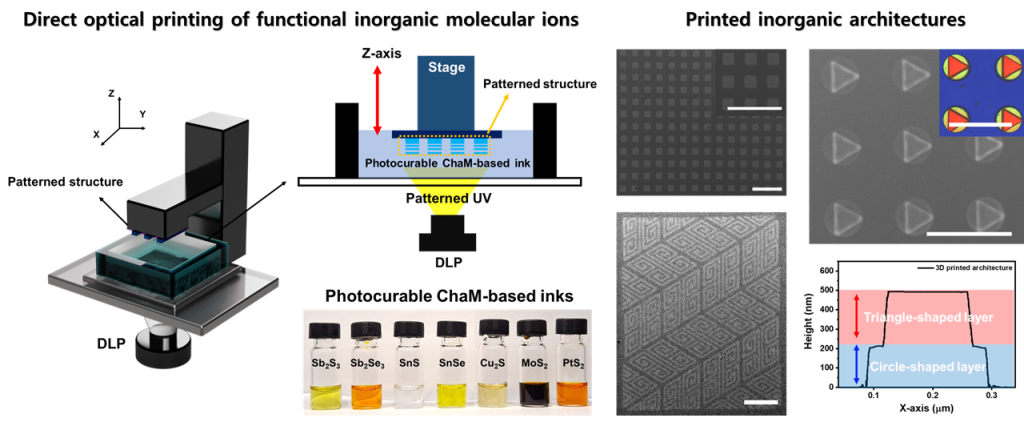
Design & Processing
Extrusion-based 3D printing
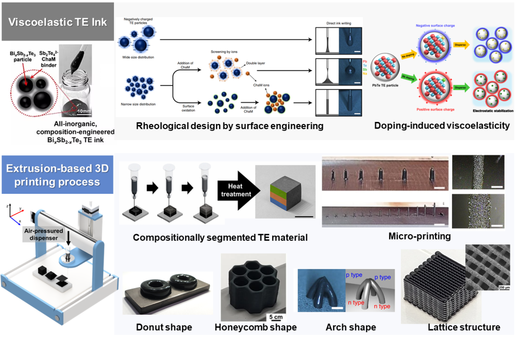
Extrusion-based additive manufacturing process is the most basic form of 3D printing which relies solely on the rheological property of the ink. These processes include dispenser printing, and robocasting. Since there is no complex constituent that is required for this printing process, the processing parameter itself is relatively simple compared to other manufacturing techniques. For dispensing printing method, the ink must exhibit non-Newtonian and viscoelastic behavior. The inks must be tailored to simultaneously have shear-thinning behavior, which facilitates reliable extrusion flow through the nozzle to prevent clogging, and high elasticity to avoid the collapse of the 3D structure.
Viscoelastic thermoelectric (TE) ink
As a model application of this processing, we focus on the development of viscoelastic inks containing TE particles. TE inks are often paired with polymer-based organic binder to give rise to viscoelastic behavior. TE performance of these composite inks with polymer matrix is strictly limited due to low power factors. TE inks with organic binder suffer from low electrical property due to its intrinsically insulating property. We are replacing the electrically insulating polymer matrix with molecular chalcogenidometallate-based (ChaM) ions, anions containing metal atoms ligated with chalcogens. We design the rheological properties of TE ink through surface engineering such as ChaM ion addition, doping, etc.
Extrusion-based 3D printing process
Our group developed extrusion-based 3D printing process for viscoelastic TE inks that enables the fabrication of TE materials into 3D shapes. In this printing process, ink is dispensed out of the nozzle directly to the substrate by pneumatic control. The printing process enables precise micro-scale 3D printing by reducing the particle size in the TE ink or the nozzle size while controlling the process parameters. This developed 3D printing process allows for increased freedom in designing TE materials and devices.
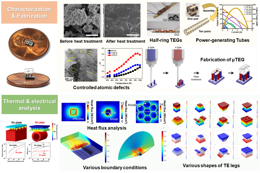
Characterization & Fabrication
We can easily check the features of TE materials such as sintered state, porosity and controlled atomic defects through nano- to micro-scale characterization such as Scanning Electron Microscopy (SEM) or Transmission Electron Microscopy (TEM). After confirming the reliability of TE materials through characterization, we can fabricate customized TE devices such as half-ring TEG, tube-shaped TEG and micro-scale TEG for different types of heat sources.
Thermal and electrical analysis
Thermal and electrical analysis plays a fundamental role in the development, optimization, and application of TE materials and devices. It allows researchers and engineers to understand the underlying principles, characterize materials, design efficient devices, and address real-world challenges, ultimately advancing the field of TEs and its diverse applications.
Relevant publication:
– Eom, et al. Rheological design of 3D printable all-inorganic inks using BiSbTe-based thermoelectric materials. J. Rheol. 2019, 63, 291-304.
– Jo, et al. Ink processing for thermoelectric materials and power generating devices. Adv. Mater. 2019, 31, 1804930.
– Kim, et al. 3D printing of shape-conformable thermoelectric materials using all-inorganic Bi2Te3-based inks. Nature Energy 2018, 3, 301-309.
– Park, et al. High performance shape-engineerable thermoelectric painting. Nature Commun. 2016, 7, 13403.
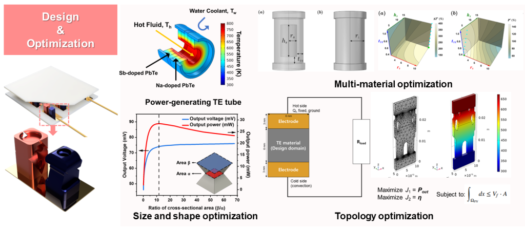
Design & Optimization
Design and optimization is critical as it tunes existing materials and devices, enhancing their performance in real-world applications. It enables engineers to maximize energy efficiency, reduce energy losses, and tailor thermoelectric systems for diverse boundary conditions. Also, optimization techniques can be divided into size, shape and topology optimization, and the variables to be designed can be expanded from single material to multi-material.
The new design principles and optimization techniques not only advances scientific understanding but also drives practical applications, potentially transforming industries by providing clean and efficient energy solutions.
Relevant publication:
– Choo, et al. Geometric design of defect-engineered Cu2Se-based thermoelectric energy harvester. submitted.
– Kim, et al. Direct ink writing of three-dimensional thermoelectric microarchitectures. Nature Electronics 2021, 4, 579-587.
– Kim, et al. 3D Printing for Energy Applications. WILEY, 2021, C.6 THERMOELECTRICS.
– Choo, et al. Cu2Se-based Thermoelectric Cellular Architectures for Efficient and Durable Power Generation. Nature Commun. 2021, 12, 3550.
– Lee, et al. Doping-Induced Viscoelasticity in PbTe Thermoelectric Inks for 3D printing of Power-Generating Tubes. Adv. Energy Mater. 2021, 11, 2100190.
Solution-processed thin films
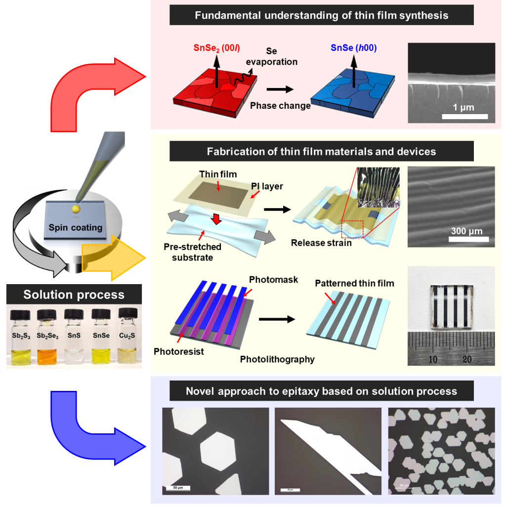
We are designing novel all-inorganic inks comprising of soluble inorganic precursors or nanocrystals for the fabrication of thin films with tailored composition, structure, and properties. The materials of interest include semiconducting metal chalcogenides and phosphorus, metallic Ag, Cu, and 2D MXenes, applied to thermoelectric,electronic, optoelectronic, energy, and flexible devices.
Relevant publication:
– Heo, et al. Thin Film and Flexible Thermoelectric Generators, Devices, and Sensors. Springer, 2021, Part I-3. Solution-Processed Metal Chalcogenide Thermoelectric Thin Films.
Nano 3D architecturing
